WORKSHOP
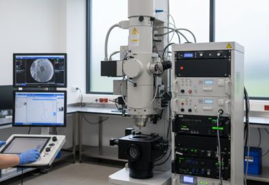
Scanning Electron Microscopy (SEM)
Launch: 15 Feb 2026, 05:00 PM
Scanning Electron Microscopy (SEM)
Workshop Highlights
Introduction and History of SEM
Principle of SEM
-
Electron beam–sample interaction
-
Secondary Electrons (SE) and Backscattered Electrons (BSE)
-
Energy Dispersive Spectroscopy (EDS) for elemental analysis
Sample Preparation Techniques
-
Fixation methods for biological and material samples
-
Coating techniques (gold, carbon)
-
Proper mounting for high-quality imaging
Case Study
Applications and Examples
Program Particulars
| Particulars | Details |
|---|
| Title | Scanning Electron Microscopy (SEM) – Workshop |
| Duration | 1 hour |
| Mode of Delivery | Online session |
| Program Fee | ₹99 (Individual Registration) |
| Deliverables | E-Certificate, Course Material |
| Target Audience | Students, Researchers, and Professionals in Nanotechnology, Materials Science, Biotechnology, Life Sciences |
- ✓ After completing this workshop, participants will be able to:
- ✓ Understand the working principle of SEM and electron–sample interactions
- ✓ Prepare different types of samples for SEM analysis
- ✓ Identify and minimize common SEM artifacts and limitations
- ✓ Perform basic troubleshooting during SEM imaging
- ✓ Analyze SEM images for research and industrial applications
Mrs.Nandhini Muthukumaran
Nanotechnologist
Founder and Director of Nano Nest Private Limited
Excels in the fabrication of nanoparticles
Expertise in characterization of nanomaterials
Skilled in curating scientific and technical workshops
Delivers complex concepts in a clear and understandable manner
Experienced in hands-on training and practical demonstrations
Strong ability to engage students, researchers, and professionals
Focused on industry-relevant and application-oriented learning